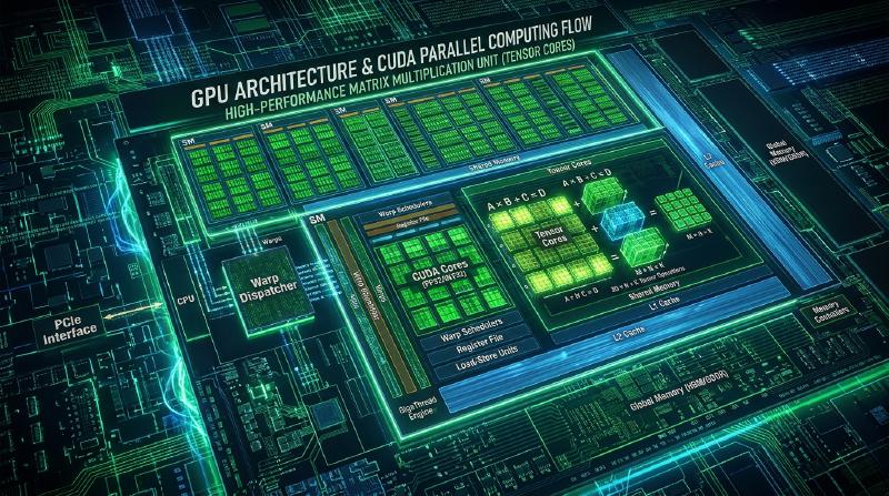
GPU’s Massively Parallel Architecture and CUDA Physics: Computational Principles of SIMT, Warps, and Tensor Cores
The foundational technology supporting modern advanced computational science, artificial intelligence, deep learning, and high-definition computer graphics is the GPU (Graphics Processing Unit). In this article, we will deeply delve into the architecture of the GPU and the physical and hardware aspects of CUDA (Compute Unified Device Architecture), the parallel computing platform that runs on it. Rather than just programming syntax, we will thoroughly dissect “why the hardware is designed the way it is” and “how it achieves extreme computational throughput” from the perspectives of Streaming Multiprocessors (SM), the SIMT execution model, warp scheduling, tensor cores, and the memory hierarchy.
Chapter 1: The Divergence in Design Philosophy Between CPU and GPU
1.1 Pursuit of Low Latency vs. Pursuit of High Throughput
The CPU (Central Processing Unit), a general-purpose processor, and the GPU, which is specialized for parallel computing, have fundamentally different design philosophies stemming from their origins. The CPU has evolved with the supreme mandate of “low latency (minimizing delay),” focusing on “how fast a single task (thread) can be finished.” On the other hand, the GPU pursues “high throughput (maximizing processing volume),” focusing on “how much processing can be completed per unit of time as a whole by bundling massive amounts of tasks.”
The CPU must swiftly handle unpredictable processes such as operating system control, application execution with complex branching conditions, and random interrupt handling from users. For this reason, it is equipped with highly advanced branch prediction circuits, out-of-order execution (a mechanism that executes instructions out of sequence), and huge L1/L2/L3 cache memories, maximizing the performance of a single thread while hiding memory access delays.
In contrast, the GPU was originally created to handle highly parallelizable tasks, such as applying the same shading calculations to millions of pixels on a screen. Rather than allocating die area to complex control circuits and huge caches, the choice was made to pack as many simple arithmetic logic units (ALUs) as possible to the absolute limit.
1.2 Die Area Allocation Ratio of Cache, Control Circuits, and ALUs
How the limited area (transistor budget) of a silicon die (semiconductor chip) is allocated determines the architectural differences between the two.
- CPU Die Area Allocation: More than half of the die is occupied by large-capacity cache memory (SRAM) and advanced control circuits (branch prediction, instruction fetch, decode, scheduling, etc.). The proportion occupied by ALUs performing actual calculations is relatively small.
- GPU Die Area Allocation: Cache memory and control circuits are kept to an absolute minimum, and the majority of the die is occupied by thousands to tens of thousands of ALUs (CUDA cores).
The GPU hides memory access delay (latency) not with caches, but through “context switching.” While one group of threads is waiting for data to arrive from memory, it immediately executes the calculations for another group of threads, keeping the calculation units constantly running (high occupancy). This is the physical implementation of the “pursuit of high throughput” in a GPU. Because Hardware Multithreading is extremely lightweight, it is predicated on the existence of thousands to tens of thousands of concurrent threads.
Chapter 2: The Essence of the SIMT Execution Model
2.1 The Difference Between SIMD and SIMT
While Flynn’s taxonomy exists as a classification of parallel processing, the GPU’s execution model is often compared to SIMD (Single Instruction, Multiple Data). CPU vector extension instructions (such as AVX) are purely SIMD, processing multiple pieces of data (e.g., eight 32-bit floating-point numbers stored in a 256-bit wide register) simultaneously with a single instruction. In SIMD, it is very difficult to execute different branches (if-else) for each element of data.
On the other hand, the execution model of CUDA advocated by NVIDIA is called SIMT (Single Instruction, Multiple Threads). In SIMT, multiple independent “threads” form a group (a “warp,” described later) and share and execute the same instruction. However, unlike SIMD, each thread in SIMT has an independent register state and instruction address counter (in the programming model). This allows programmers to write code as if each thread were operating independently.
2.2 The 32-Thread “Warp”
GPU hardware does not schedule threads individually; it manages and executes them in units called “warps,” which bundle 32 threads together. (AMD GPUs call this a Wavefront, and sometimes 64-thread units are adopted).
The instruction fetch/decode unit inside a Streaming Multiprocessor (SM) fetches one instruction per warp and issues (dispatches) the same instruction to all 32 threads in the warp. That is, the 32 threads in a warp physically execute the exact same instruction simultaneously on their respective different data. This is the core of SIMT.
2.3 The Physical Penalty of Warp Divergence
Even though each thread can behave as if it has an independent program counter, physically all threads in a warp must execute the same instruction. So, what happens if there is a conditional branch like if-else in the code, and the truth value of the branch condition differs among the threads in the warp?
This phenomenon is called Warp Divergence.
When warp divergence occurs, the hardware processes it in the following steps:
- First, it executes the instruction only for the threads where the
ifcondition was true (active threads). At this time, the threads where the condition was false are “masked” (disabled), and the calculation results are not written. - Next, it transitions to the
elsecondition (or the path when the condition is false), activates the threads that were masked earlier, masks the threads that were true, and executes the instruction.
In other words, when there are multiple branch paths, the hardware is forced to execute those paths serially, not in parallel. As an extreme example, if 32 threads in a warp take 32 different branch paths, the execution time jumps by 32 times. Warp divergence is one of the biggest factors drastically reducing the computational throughput of a GPU and is an anti-pattern that must be avoided above all in algorithm design. Physically, it means that even though the ALU is consuming power, “wasted cycles” occur where valid calculation results are not being generated because it is masked.
Chapter 3: Hardware Anatomy of the Streaming Multiprocessor (SM)
A GPU is constructed as a collection of numerous Streaming Multiprocessors (SMs). The SM is the true computation engine of the GPU. In modern architectures (e.g., Hopper H100), over 100 SMs are mounted on a single GPU die.
3.1 Pipeline Structure Inside the SM
An SM is internally further divided into multiple sub-partitions (usually four), each with an independent warp scheduler and dispatch unit.
- Warp Scheduler: Selects warps that are in an executable state (registers and memory are ready). The GPU scheduler can switch warps with zero overhead, which is the key to hiding memory access latency.
- Dispatch Unit: Issues instructions to scheduled warps.
- CUDA Cores (INT32 / FP32 / FP64 ALU): Units that perform actual integer and floating-point arithmetic.
- Load/Store Unit (LD/ST Unit): Handles reading from and writing to memory.
- Special Function Unit (SFU): Dedicated hardware for rapidly calculating transcendental functions such as sin, cos, exp, and reciprocals.
The instruction pipeline is designed to be very deep, with stages for fetch, decode, scheduling, register read, execution (multiple cycles), and write-back. The latency of an FP32 FMA (Fused Multiply-Add) calculation normally takes several to a dozen cycles, but by issuing instructions from a different warp every cycle, the pipeline is constantly kept full.
3.2 Huge Register Files and Register Pressure
SMs are equipped with register files that are incomparably huge compared to CPUs (e.g., 64KB to 256KB of SRAM per SM). This is to hold all the contexts of thousands of threads executed concurrently on the SM.
Context switches are completed in zero cycles because there is no need to save (spill) the register state of a thread to memory. However, as the number of registers used per thread increases, the number of warps that can be launched simultaneously in an SM (occupancy) decreases. This is called register pressure. When registers run out, data is spilled to slow local memory (physically part of global memory), causing a devastating performance drop.
3.3 Shared Memory and Bank Conflicts
SMs have Shared Memory, which is ultra-fast on-chip memory explicitly controllable by the programmer. It shares the same physical SRAM region as the L1 cache but functions as an explicit data cache, used for data sharing and synchronization among threads within a block.
The physical structure of shared memory is divided into multiple independent modules (usually 32) called Memory Banks. Consecutive 32-bit addresses are interleaved (allocated) to different banks.
When 32 threads in a warp simultaneously access different banks, the accesses are processed completely in parallel (in 1 cycle). This is called bank-conflict-free. However, if multiple threads try to access different addresses in the same bank simultaneously, the requests are serialized, and a penalty (delay) occurs. This is called a Bank Conflict. For example, a 2-way bank conflict doubles the access time, and in the worst case, a 32-way conflict delays it by 32 times. In algorithms like matrix transposition, stride access causes severe bank conflicts, so advanced optimization using padding (a technique of inserting dummy data to shift memory addresses) is essential to avoid conflicts.
Chapter 4: The Multiply-Accumulate Pipeline of the Tensor Core
First introduced in the Volta architecture, the revolutionary hardware that dramatically boosted GPU performance thereafter is the Tensor Core. The explosive development of AI and deep learning cannot be discussed without tensor cores.
4.1 Hardware Implementation of Matrix Multiply-Accumulate (MMA)
The majority of deep learning computations are matrix multiplications (GEMM: General Matrix Multiply) between a neural network’s weight matrix and the input data matrix. The formula is expressed as $D = A \times B + C$ ($A$ and $B$ are input matrices, $C$ is the accumulator matrix).
In conventional CUDA cores, this matrix multiplication was calculated element by element using FMA (Fused Multiply-Add) instructions. In contrast, a tensor core is a dedicated circuit that executes matrix multiply-accumulate operations for small matrices (e.g., 4x4 or 16x16) at the hardware level in a single cycle (or just a few cycles).
Physically, dozens to hundreds of multipliers and huge addition trees are directly connected by wires, completing the multiply-accumulate operation all at once without writing intermediate results back to registers. Because of this, the computational throughput per area (TFLOPS) is orders of magnitude higher compared to standard CUDA cores.
4.2 The Secret of Mixed-Precision
Another essence of tensor cores is their support for Mixed-Precision calculations. In deep learning, there are many situations where high precision (FP32/FP64) is not required during the computation process. Tensor cores have a pipeline that reads input matrices $A$ and $B$ in low precision (FP16, BF16, or even lower FP8, INT8, INT4), performs internal multiplication in low precision, and then performs the addition (accumulate) process in higher precision (FP32 or INT32).
- FP16 / BF16: The standard for training. BF16 (Bfloat16) has the same 8-bit exponent as FP32, providing a wide dynamic range and making it easier to prevent vanishing gradients.
- FP8 / INT8 / INT4: The trump cards for accelerating inference. Because the amount of data transfer (memory bandwidth) is also reduced, throughput improves dramatically.
In the Hopper architecture, “FP8 Tensor Cores,” which dramatically accelerate Transformer model calculations, have been introduced, theoretically achieving dozens of times the throughput compared to FP32. From the software side (CUDA), tensor cores are directly driven through wmma (Warp-Level Matrix Multiply and Accumulate) APIs or mma.sync PTX instructions, performing extremely complex collective processing where threads in a warp cooperate to load, compute, and store matrix fragments into registers.
Chapter 5: CUDA Memory Hierarchy and Optimization Techniques
No matter how high a GPU’s computational power is, if data supply becomes a bottleneck, performance will not be achieved (the memory wall problem). It is no exaggeration to say that 90% of optimization in CUDA programming is “memory access optimization.”
5.1 Global Memory Coalesced Access
Global memory, which is the main memory of the GPU (HBM or GDDR), has a very wide bandwidth (e.g., several TB/s) but also a very high latency of hundreds of cycles.
The absolute principle for maximizing global memory access efficiency is Coalescing. The GPU’s memory controller accesses memory in transactions of 32-byte, 64-byte, or 128-byte units. When the 32 threads in a warp access memory, if their memory addresses fall within a contiguous region (aligned 128-byte boundary), the hardware combines (coalesces) these requests into a single memory transaction to process them.
Conversely, if threads access random addresses or perform strided (spaced apart) accesses, combining does not occur, and multiple transactions are generated. This is called “uncoalesced access,” and it is a fatal performance bug that reduces effective memory bandwidth to less than a tenth.
5.2 CUDA C++ Code Example: Matrix Transpose Optimization and Shared Memory
Below is an example of an optimized kernel code for Matrix Transpose that dramatically improves performance by avoiding uncoalesced access and utilizing shared memory.
| |
There are three key points in this code:
- Coalescing during read: The read from
idatais done in the X direction wherethreadIdx.xis contiguous, so it is fully coalesced. - Coalescing during write: The write to
odatais also designed to be contiguous in thethreadIdx.xdirection by swapping the block coordinates, ensuring it is coalesced. - Padding in shared memory: By shifting by one element (padding) with
tile[TILE_DIM][TILE_DIM + 1], bank conflicts when accessing in the column direction (tile[threadIdx.x][threadIdx.y + j]) during writes are completely eliminated.
5.3 Cache Hierarchy and Special Memory
- L1/L2 Cache Policies: In recent GPU architectures, programmers can control cache behavior as hints using PTX instructions (such as
.ca,.cg,.cs). For example, data that will only be accessed once can bypass the L2 cache (streaming access), preventing cache pollution. - Texture Memory / Constant Memory: Texture memory, specialized for image processing, utilizes dedicated caches for accesses with 2D spatial locality. Constant memory boasts extremely high efficiency for broadcast accesses where all threads read the same constant.
Chapter 6: The Future of GPUs in the Deep Learning Era
Scaling the overall system, rather than just improving the performance of a single GPU, is the current frontier of computational science.
6.1 Ultra-High-Speed Interconnection via NVLink and NVSwitch
Huge LLMs (Large Language Models) cannot fit in the memory of a single GPU (e.g., 80GB or 144GB). To perform model parallelism (tensor parallel or pipeline parallel), terabytes of data per second must be exchanged between GPUs. Because traditional PCIe (PCI Express) buses cannot cover this bandwidth, NVIDIA developed a proprietary high-speed interconnect called NVLink. Furthermore, through switch chips called NVSwitch, 8 or 256 GPUs can be connected via a completely non-blocking crossbar switch, allowing the construction of clusters that behave as if they were one giant GPU.
6.2 Transformer Engine and the FP8 Ecosystem
To optimize not only for natural language processing but also for the Transformer architecture, which has become the de facto standard in image and speech recognition, the Hopper architecture introduced a hardware-software cooperative mechanism called the Transformer Engine. This dynamically monitors the statistical information of tensors and automatically switches the computation precision between FP8 and FP16 layer by layer (Dynamic Scaling), realizing extreme calculation speeds and memory bandwidth savings while preventing precision degradation.
6.3 GPU Cluster Scaling Laws and Future Prospects
As OpenAI’s “Scaling Laws” show, the more the number of model parameters and computational volume are increased, the more AI performance continues to improve. Along with this, GPUs are evolving from mere processors into “entire data centers acting as one giant GPU (supercomputer)” with tens of thousands of units connected by optical fiber.
Future architectural evolutions will likely head toward the introduction of silicon photonics (optical interconnects), CPO (Co-Packaged Optics), and further advancements in 3D stacking technology from SRAM to HBM. However, the unchanging DNA from the moment GPUs were born—“maximizing throughput through parallel processing”—will continue to pioneer the forefront of computational science.
[Additional Discussion] Mathematical Analysis of Scheduling and Occupancy in GPUs
title: “Graphics Processing Unit’s Massively Parallel Architecture and CUDA Physics: Computational Principles of SIMT, Warps, and Tensor Cores” description: “The internal design of graphics processing units pushing for extreme high throughput. The essence of SM, warp scheduling, tensor cores, and shared memory optimization.” slug: “gpu-architecture-cuda-parallel-computing” date: “2026-10-03T05:00:00+09:00” categories: [“architecture”, “technology”] tags: [“gpu”, “cuda”, “parallel-computing”, “hardware”] image: “eyecatch.jpg”
Graphics Processing Unit’s Massively Parallel Architecture and CUDA Physics: Computational Principles of SIMT, Warps, and Tensor Cores
The foundational technology supporting modern advanced computational science, artificial intelligence, deep learning, and high-definition computer graphics is the Graphics Processing Unit. In this article, we will deeply delve into the architecture of the graphics processing unit and the physical and hardware aspects of CUDA (Compute Unified Device Architecture), the parallel computing platform that runs on it. Rather than just programming syntax, we will thoroughly dissect “why the hardware is designed the way it is” and “how it achieves extreme computational throughput” from the perspectives of Streaming Multiprocessors (SM), the SIMT execution model, warp scheduling, tensor cores, and the memory hierarchy.
Supplement Chapter 1: The Divergence in Design Philosophy Between General-Purpose Processors and Graphics Processing Units
1.1 Pursuit of Low Latency vs. Pursuit of High Throughput
The general-purpose processor (Central Processing Unit) and the graphics processing unit, which is specialized for parallel computing, have fundamentally different design philosophies stemming from their origins. The general-purpose processor has evolved with the supreme mandate of “low latency (minimizing delay),” focusing on “how fast a single task (thread) can be finished.” On the other hand, the graphics processing unit pursues “high throughput (maximizing processing volume),” focusing on “how much processing can be completed per unit of time as a whole by bundling massive amounts of tasks.”
The general-purpose processor must swiftly handle unpredictable processes such as operating system control, application execution with complex branching conditions, and random interrupt handling from users. For this reason, it is equipped with highly advanced branch prediction circuits, out-of-order execution (a mechanism that executes instructions out of sequence), and huge L1/L2/L3 cache memories, maximizing the performance of a single thread while hiding memory access delays.
In contrast, the graphics processing unit was originally created to handle highly parallelizable tasks, such as applying the same shading calculations to millions of pixels on a screen. Rather than allocating die area to complex control circuits and huge caches, the choice was made to pack as many simple arithmetic logic units (ALUs) as possible to the absolute limit.
1.2 Die Area Allocation Ratio of Cache, Control Circuits, and ALUs
How the limited area (transistor budget) of a silicon die (semiconductor chip) is allocated determines the architectural differences between the two.
- General-Purpose Processor Die Area Allocation: More than half of the die is occupied by large-capacity cache memory (SRAM) and advanced control circuits (branch prediction, instruction fetch, decode, scheduling, etc.). The proportion occupied by ALUs performing actual calculations is relatively small.
- Graphics Processing Unit Die Area Allocation: Cache memory and control circuits are kept to an absolute minimum, and the majority of the die is occupied by thousands to tens of thousands of ALUs (CUDA cores).
The graphics processing unit hides memory access delay (latency) not with caches, but through “context switching.” While one group of threads is waiting for data to arrive from memory, it immediately executes the calculations for another group of threads, keeping the calculation units constantly running (high occupancy). This is the physical implementation of the “pursuit of high throughput” in a graphics processing unit. Because Hardware Multithreading is extremely lightweight, it is predicated on the existence of thousands to tens of thousands of concurrent threads.
Supplement Chapter 2: The Essence of the SIMT Execution Model
2.1 The Difference Between SIMD and SIMT
While Flynn’s taxonomy exists as a classification of parallel processing, the graphics processing unit’s execution model is often compared to SIMD (Single Instruction, Multiple Data). General-purpose processor vector extension instructions (such as AVX) are purely SIMD, processing multiple pieces of data (e.g., eight 32-bit floating-point numbers stored in a 256-bit wide register) simultaneously with a single instruction. In SIMD, it is very difficult to execute different branches (if-else) for each element of data.
On the other hand, the execution model of CUDA advocated by NVIDIA is called SIMT (Single Instruction, Multiple Threads). In SIMT, multiple independent “threads” form a group (a “warp,” described later) and share and execute the same instruction. However, unlike SIMD, each thread in SIMT has an independent register state and instruction address counter (in the programming model). This allows programmers to write code as if each thread were operating independently.
2.2 The 32-Thread “Warp”
Graphics processing unit hardware does not schedule threads individually; it manages and executes them in units called “warps,” which bundle 32 threads together. (AMD graphics processing units call this a Wavefront, and sometimes 64-thread units are adopted).
The instruction fetch/decode unit inside a Streaming Multiprocessor (SM) fetches one instruction per warp and issues (dispatches) the same instruction to all 32 threads in the warp. That is, the 32 threads in a warp physically execute the exact same instruction simultaneously on their respective different data. This is the core of SIMT.
2.3 The Physical Penalty of Warp Divergence
Even though each thread can behave as if it has an independent program counter, physically all threads in a warp must execute the same instruction. So, what happens if there is a conditional branch like if-else in the code, and the truth value of the branch condition differs among the threads in the warp?
This phenomenon is called Warp Divergence.
When warp divergence occurs, the hardware processes it in the following steps:
- First, it executes the instruction only for the threads where the
ifcondition was true (active threads). At this time, the threads where the condition was false are “masked” (disabled), and the calculation results are not written. - Next, it transitions to the
elsecondition (or the path when the condition is false), activates the threads that were masked earlier, masks the threads that were true, and executes the instruction.
In other words, when there are multiple branch paths, the hardware is forced to execute those paths serially, not in parallel. As an extreme example, if 32 threads in a warp take 32 different branch paths, the execution time jumps by 32 times. Warp divergence is one of the biggest factors drastically reducing the computational throughput of a graphics processing unit and is an anti-pattern that must be avoided above all in algorithm design. Physically, it means that even though the ALU is consuming power, “wasted cycles” occur where valid calculation results are not being generated because it is masked.
Supplement Chapter 3: Hardware Anatomy of the Streaming Multiprocessor (SM)
A graphics processing unit is constructed as a collection of numerous Streaming Multiprocessors (SMs). The SM is the true computation engine of the graphics processing unit. In modern architectures (e.g., Hopper H100), over 100 SMs are mounted on a single graphics processing unit die.
3.1 Pipeline Structure Inside the SM
An SM is internally further divided into multiple sub-partitions (usually four), each with an independent warp scheduler and dispatch unit.
- Warp Scheduler: Selects warps that are in an executable state (registers and memory are ready). The graphics processing unit scheduler can switch warps with zero overhead, which is the key to hiding memory access latency.
- Dispatch Unit: Issues instructions to scheduled warps.
- CUDA Cores (INT32 / FP32 / FP64 ALU): Units that perform actual integer and floating-point arithmetic.
- Load/Store Unit (LD/ST Unit): Handles reading from and writing to memory.
- Special Function Unit (SFU): Dedicated hardware for rapidly calculating transcendental functions such as sin, cos, exp, and reciprocals.
The instruction pipeline is designed to be very deep, with stages for fetch, decode, scheduling, register read, execution (multiple cycles), and write-back. The latency of an FP32 FMA (Fused Multiply-Add) calculation normally takes several to a dozen cycles, but by issuing instructions from a different warp every cycle, the pipeline is constantly kept full.
3.2 Huge Register Files and Register Pressure
SMs are equipped with register files that are incomparably huge compared to general-purpose processors (e.g., 64KB to 256KB of SRAM per SM). This is to hold all the contexts of thousands of threads executed concurrently on the SM.
Context switches are completed in zero cycles because there is no need to save (spill) the register state of a thread to memory. However, as the number of registers used per thread increases, the number of warps that can be launched simultaneously in an SM (occupancy) decreases. This is called register pressure. When registers run out, data is spilled to slow local memory (physically part of global memory), causing a devastating performance drop.
3.3 Shared Memory and Bank Conflicts
SMs have Shared Memory, which is ultra-fast on-chip memory explicitly controllable by the programmer. It shares the same physical SRAM region as the L1 cache but functions as an explicit data cache, used for data sharing and synchronization among threads within a block.
The physical structure of shared memory is divided into multiple independent modules (usually 32) called Memory Banks. Consecutive 32-bit addresses are interleaved (allocated) to different banks.
When 32 threads in a warp simultaneously access different banks, the accesses are processed completely in parallel (in 1 cycle). This is called bank-conflict-free. However, if multiple threads try to access different addresses in the same bank simultaneously, the requests are serialized, and a penalty (delay) occurs. This is called a Bank Conflict. For example, a 2-way bank conflict doubles the access time, and in the worst case, a 32-way conflict delays it by 32 times. In algorithms like matrix transposition, stride access causes severe bank conflicts, so advanced optimization using padding (a technique of inserting dummy data to shift memory addresses) is essential to avoid conflicts.
Supplement Chapter 4: The Multiply-Accumulate Pipeline of the Tensor Core
First introduced in the Volta architecture, the revolutionary hardware that dramatically boosted graphics processing unit performance thereafter is the Tensor Core. The explosive development of AI and deep learning cannot be discussed without tensor cores.
4.1 Hardware Implementation of Matrix Multiply-Accumulate (MMA)
The majority of deep learning computations are matrix multiplications (GEMM: General Matrix Multiply) between a neural network’s weight matrix and the input data matrix. The formula is expressed as $D = A \times B + C$ ($A$ and $B$ are input matrices, $C$ is the accumulator matrix).
In conventional CUDA cores, this matrix multiplication was calculated element by element using FMA (Fused Multiply-Add) instructions. In contrast, a tensor core is a dedicated circuit that executes matrix multiply-accumulate operations for small matrices (e.g., 4x4 or 16x16) at the hardware level in a single cycle (or just a few cycles).
Physically, dozens to hundreds of multipliers and huge addition trees are directly connected by wires, completing the multiply-accumulate operation all at once without writing intermediate results back to registers. Because of this, the computational throughput per area (TFLOPS) is orders of magnitude higher compared to standard CUDA cores.
4.2 The Secret of Mixed-Precision
Another essence of tensor cores is their support for Mixed-Precision calculations. In deep learning, there are many situations where high precision (FP32/FP64) is not required during the computation process. Tensor cores have a pipeline that reads input matrices $A$ and $B$ in low precision (FP16, BF16, or even lower FP8, INT8, INT4), performs internal multiplication in low precision, and then performs the addition (accumulate) process in higher precision (FP32 or INT32).
- FP16 / BF16: The standard for training. BF16 (Bfloat16) has the same 8-bit exponent as FP32, providing a wide dynamic range and making it easier to prevent vanishing gradients.
- FP8 / INT8 / INT4: The trump cards for accelerating inference. Because the amount of data transfer (memory bandwidth) is also reduced, throughput improves dramatically.
In the Hopper architecture, “FP8 Tensor Cores,” which dramatically accelerate Transformer model calculations, have been introduced, theoretically achieving dozens of times the throughput compared to FP32. From the software side (CUDA), tensor cores are directly driven through wmma (Warp-Level Matrix Multiply and Accumulate) APIs or mma.sync PTX instructions, performing extremely complex collective processing where threads in a warp cooperate to load, compute, and store matrix fragments into registers.
Supplement Chapter 5: CUDA Memory Hierarchy and Optimization Techniques
No matter how high a graphics processing unit’s computational power is, if data supply becomes a bottleneck, performance will not be achieved (the memory wall problem). It is no exaggeration to say that 90% of optimization in CUDA programming is “memory access optimization.”
5.1 Global Memory Coalesced Access
Global memory, which is the main memory of the graphics processing unit (HBM or GDDR), has a very wide bandwidth (e.g., several TB/s) but also a very high latency of hundreds of cycles.
The absolute principle for maximizing global memory access efficiency is Coalescing. The graphics processing unit’s memory controller accesses memory in transactions of 32-byte, 64-byte, or 128-byte units. When the 32 threads in a warp access memory, if their memory addresses fall within a contiguous region (aligned 128-byte boundary), the hardware combines (coalesces) these requests into a single memory transaction to process them.
Conversely, if threads access random addresses or perform strided (spaced apart) accesses, combining does not occur, and multiple transactions are generated. This is called “uncoalesced access,” and it is a fatal performance bug that reduces effective memory bandwidth to less than a tenth.
5.2 CUDA C++ Code Example: Matrix Transpose Optimization and Shared Memory
Below is an example of an optimized kernel code for Matrix Transpose that dramatically improves performance by avoiding uncoalesced access and utilizing shared memory.
| |
There are three key points in this code:
- Coalescing during read: The read from
idatais done in the X direction wherethreadIdx.xis contiguous, so it is fully coalesced. - Coalescing during write: The write to
odatais also designed to be contiguous in thethreadIdx.xdirection by swapping the block coordinates, ensuring it is coalesced. - Padding in shared memory: By shifting by one element (padding) with
tile[TILE_DIM][TILE_DIM + 1], bank conflicts when accessing in the column direction (tile[threadIdx.x][threadIdx.y + j]) during writes are completely eliminated.
5.3 Cache Hierarchy and Special Memory
- L1/L2 Cache Policies: In recent graphics processing unit architectures, programmers can control cache behavior as hints using PTX instructions (such as
.ca,.cg,.cs). For example, data that will only be accessed once can bypass the L2 cache (streaming access), preventing cache pollution. - Texture Memory / Constant Memory: Texture memory, specialized for image processing, utilizes dedicated caches for accesses with 2D spatial locality. Constant memory boasts extremely high efficiency for broadcast accesses where all threads read the same constant.
Supplement Chapter 6: The Future of Graphics Processing Units in the Deep Learning Era
Scaling the overall system, rather than just improving the performance of a single graphics processing unit, is the current frontier of computational science.
6.1 Ultra-High-Speed Interconnection via NVLink and NVSwitch
Huge LLMs (Large Language Models) cannot fit in the memory of a single graphics processing unit (e.g., 80GB or 144GB). To perform model parallelism (tensor parallel or pipeline parallel), terabytes of data per second must be exchanged between graphics processing units. Because traditional PCIe (PCI Express) buses cannot cover this bandwidth, NVIDIA developed a proprietary high-speed interconnect called NVLink. Furthermore, through switch chips called NVSwitch, 8 or 256 graphics processing units can be connected via a completely non-blocking crossbar switch, allowing the construction of clusters that behave as if they were one giant graphics processing unit.
6.2 Transformer Engine and the FP8 Ecosystem
To optimize not only for natural language processing but also for the Transformer architecture, which has become the de facto standard in image and speech recognition, the Hopper architecture introduced a hardware-software cooperative mechanism called the Transformer Engine. This dynamically monitors the statistical information of tensors and automatically switches the computation precision between FP8 and FP16 layer by layer (Dynamic Scaling), realizing extreme calculation speeds and memory bandwidth savings while preventing precision degradation.
6.3 Graphics Processing Unit Cluster Scaling Laws and Future Prospects
As OpenAI’s “Scaling Laws” show, the more the number of model parameters and computational volume are increased, the more AI performance continues to improve. Along with this, graphics processing units are evolving from mere processors into “entire data centers acting as one giant graphics processing unit (supercomputer)” with tens of thousands of units connected by optical fiber.
Future architectural evolutions will likely head toward the introduction of silicon photonics (optical interconnects), CPO (Co-Packaged Optics), and further advancements in 3D stacking technology from SRAM to HBM. However, the unchanging DNA from the moment graphics processing units were born—“maximizing throughput through parallel processing”—will continue to pioneer the forefront of computational science.
Conclusion: To the Zenith of Computational Science
The architecture of the GPU is the most complex and most throughput-focused computational engine humanity has ever created. If a CPU is a “single, ultra-high-performance Formula 1 car,” a GPU can be likened to a “massive logistics system where tens of thousands of dump trucks move materials simultaneously in a coordinated manner.”
Instruction execution in warp units via SIMT, hardware scheduling that switches thousands of threads in zero cycles, coalesced access that extracts bandwidth to the limit, and the tensor core pipeline that drove deep learning breakthroughs. All of these are the crystallized obsession—almost madness—of engineers attempting to “maximize the total volume of floating-point calculations within the limits of physical laws (the speed of light, heat, power, and the limits of silicon miniaturization).”
For software engineers, AI researchers, and HPC researchers of the future, understanding GPU architecture is not merely a matter of general knowledge. It is a “required subject” for intuitively grasping what is happening behind frameworks (like PyTorch and TensorFlow) and pushing the hardware’s capabilities to the absolute limit. Avoiding memory bank conflicts, eliminating warp divergence, and keeping the tensor core pipeline constantly full of data. At the end of such optimizations, the future—where calculations that once took months on supercomputers are now completed in hours on a few GPUs sitting on a desk—has already become a reality.
We are now living in the golden age of the most exciting computer architecture in human history. The person to understand the essence of CUDA physics and the GPU’s massively parallel architecture and give birth to the next generation of innovation might be you, reading this article right now.
Glossary
- SM (Streaming Multiprocessor): The main computation block of a GPU. Equivalent to a core in a CPU, but contains numerous CUDA cores, warp schedulers, shared memory, etc., inside it.
- SIMT (Single Instruction, Multiple Threads): A GPU-specific execution model where all threads in a warp share the same instruction while calculating on independent data.
- Warp: A collection of 32 threads. The smallest unit of hardware scheduling and instruction issuing.
- Warp Divergence: A phenomenon where branch conditions split among threads in a warp, causing the execution paths to serialize and reducing throughput.
- Tensor Core: A dedicated circuit that processes matrix multiply-accumulate (MMA) operations at once at the hardware level. Specialized for accelerating deep learning.
- Coalesced Access: A mechanism where the hardware combines memory accesses into a single transaction to achieve high bandwidth when threads in a warp access contiguous memory addresses.
- Shared Memory: Ultra-fast L1 scratchpad memory explicitly controllable by programmers, embedded inside the SM.
- Bank Conflict: A penalty in shared memory where multiple threads simultaneously access different addresses in the same bank, serializing the accesses.
- Occupancy: The actual ratio of the number of active warps on an SM to its theoretical maximum. The higher it is, the easier it is to hide memory access latency.
- Register Spilling: A phenomenon where the number of registers used by a thread exceeds the hardware limit, and overflowed data is saved to slower memory (local memory).
References and Recommended Reading List
- NVIDIA CUDA C++ Programming Guide: The official document every CUDA programmer must read. It comprehensively covers memory access patterns and optimization best practices.
- NVIDIA Ampere / Hopper Architecture Whitepaper: Official whitepapers detailing the tensor core pipeline, asynchronous memory transfers, and the hardware implementation of the Transformer Engine.
- Computer Architecture: A Quantitative Approach (John L. Hennessy, David A. Patterson): A classic masterpiece of computer architecture. Deeply explains the differences in design philosophies between CPUs and GPUs, cache hierarchies, and instruction-level parallelism.
- Programming Massively Parallel Processors: A Hands-on Approach (David B. Kirk, Wen-mei W. Hwu): A textbook explaining CUDA programming from the perspective of algorithm design. It details implementations like shared memory tiling techniques, reductions, and prefix sums.
- Dissecting the NVIDIA Volta GPU Architecture via Microbenchmarking: An academic paper. A masterpiece that unravels cache latencies and exact tensor core throughputs, which NVIDIA has not published, through microbenchmarks.
While the architectural knowledge explained in this article may become somewhat obsolete as hardware evolves, the fundamental physical principle of “maximizing bandwidth, extracting parallelism, and hiding latency” will remain a universal truth in computer science.