Introduction: The Physics of Electron Beams and the Quest for Quantum Beams Opening the Door to the Ultra-Microscopic World
Humanity’s fundamental curiosity to “see the invisible” has walked hand in hand with the history of microscopes as optical instruments. Since Antonie van Leeuwenhoek discovered microorganisms with his handmade single-lens microscope in the 17th century, the optical microscope has brought immense revolutions to biology, materials science, and natural sciences as a whole. However, entering the 20th century, as the frontier of science followed the path of miniaturization from cells to molecules, and then to atoms, observation using light faced a physical wall. That is the “Abbe diffraction limit.”
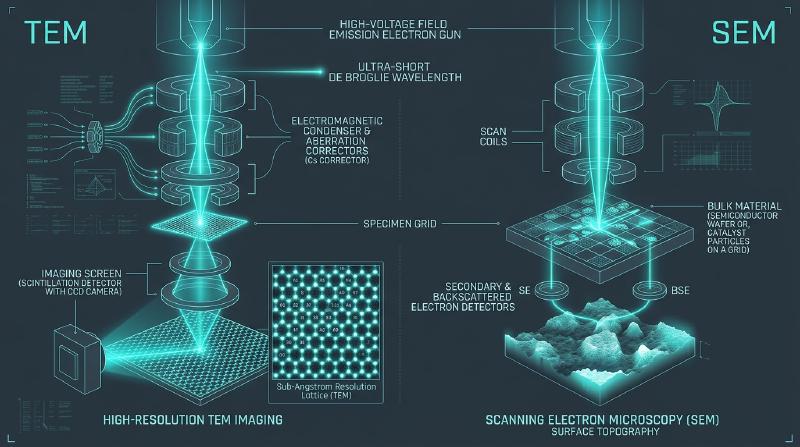
In this article, we will thoroughly explain the ultra-microscopic imaging technology of electron microscopes (Scanning Electron Microscope: SEM, Transmission Electron Microscope: TEM), which broke through the limits of optical microscopes and achieved the visualization of individual atoms. We will cover the underlying quantum mechanics, electromagnetism, and the cutting-edge spherical aberration correction technology, incorporating mathematical approaches. The process of treating an elementary particle like an electron as a quantum mechanical wave, controlling it with electromagnetic fields to form an image, can be said to be one of the most beautiful crystallizations of physical engineering that humanity has ever achieved.
Chapter 1: The Limit of Optical Microscopes and de Broglie’s Leap: The Dawn of Wave Nature and Quantum Mechanics
1.1 Abbe’s Diffraction Limit: Physical Constraints of the Wave Nature of Light and Spatial Frequency
In optical imaging, behind the act of our “seeing an object,” there is a process of spatial Fourier transform that reconstructs the wavefront of light scattered and diffracted by the object using a lens system. In 1873, the German physicist Ernst Abbe formulated the imaging mechanism of a microscope as a diffraction phenomenon. When a plane wave of wavelength $\lambda$ is incident on an object (e.g., a diffraction grating with period $d$), the light is diffracted at various angles $\theta$. The minimum condition for imaging is that, in addition to the 0th-order wave traveling straight, at least the 1st-order diffracted wave is captured by the pupil (aperture) of the objective lens, causing interference.
In the basic diffraction equation $d \sin \theta = n\lambda$, considering the 1st-order diffraction ($n=1$), the resolution is determined by the maximum angle the lens can capture (related to the numerical aperture $NA = n \sin \theta$). Abbe’s formula for the diffraction limit is as follows:
$$ d = \frac{\lambda}{2NA} $$Here, $d$ is the resolution (the minimum distance at which two points can be distinguished), $\lambda$ is the wavelength of the light used, and $NA$ is the numerical aperture of the objective lens. More strictly, based on the Rayleigh criterion as the radius of the Airy disk for a circular aperture, the resolution $\delta$ is expressed as $\delta = 0.61 \frac{\lambda}{NA}$. In either formulation, the limit is proportional to the wavelength $\lambda$ and inversely proportional to the numerical aperture $NA$, representing an absolute law of nature.
In normal air (refractive index of medium $n \approx 1$), the $NA$ is at most less than 1, and even using an oil immersion lens ($n \approx 1.5$), it is limited to about 1.4. Since the wavelength $\lambda$ of visible light is roughly 400 nm (violet) to 700 nm (red), even if light with the shortest wavelength of 400 nm and the highest performance oil immersion lens (NA = 1.4) are used, the resolution $d$ is only about 200 nm. Viruses with sizes of several thousand angstroms (1 $\text{\AA} = 0.1 \text{nm}$), smaller protein molecules (several nm), and atoms (about 0.1 nm to 0.3 nm) can absolutely never be “seen” with visible light, no matter how much the lens is polished. Attempts have been made to increase the refractive index $n$ of the medium to the extreme (such as liquid immersion lenses or solid immersion lenses), but due to the nature of electromagnetic waves, it is theoretically impossible to cross the barrier of a few thousand angstroms.
1.2 De Broglie’s Matter Waves and the Quantum Mechanical Approach
The key to breaking down this desperate wall came from a completely unexpected direction. In 1924, French physicist Louis de Broglie proposed the hypothesis of “matter waves (de Broglie waves),” stating that if light has a wave-particle duality, matter particles with mass, such as electrons, should also possess wave nature. From the analogy of Einstein’s light quantum hypothesis $E = h\nu$ and the special theory of relativity $E = mc^2$, the wavelength $\lambda$ of a de Broglie wave is inversely proportional to the particle’s momentum $p$ (the product of mass $m$ and velocity $v$), and is expressed using Planck’s constant $h$ as follows:
$$ \lambda = \frac{h}{p} = \frac{h}{mv} $$When an electron is accelerated in an electric field with a potential difference $V$ (accelerating voltage), the kinetic energy $E_k$ obtained by the electron is $E_k = eV$, where $e$ is the electron charge. In the non-relativistic region, the relationship between kinetic energy and momentum is $E_k = \frac{p^2}{2m}$, so the momentum $p$ is $p = \sqrt{2meV}$. By substituting this into the de Broglie wavelength equation, the wavelength of the electron can be calculated as follows:
$$ \lambda = \frac{h}{\sqrt{2meV}} $$1.3 Strict Derivation of Accelerating Voltage and Electron Wavelength with Relativistic Correction
In an actual transmission electron microscope (TEM), extremely high accelerating voltages ranging from tens of kV to several thousand kV are used. For instance, the velocity of an electron accelerated at 200 kV reaches about 70% of the speed of light, and at 300 kV, it reaches about 78%. In such an ultra-high-speed region, the mass increase effect due to the special theory of relativity (Lorentz factor $\gamma = \frac{1}{\sqrt{1 - v^2/c^2}}$) cannot be ignored, and classical mechanics equations will produce serious errors.
$$ E = E_k + m_0 c^2 = eV + m_0 c^2 $$$$ E^2 = (pc)^2 + (m_0 c^2)^2 $$$$ (eV + m_0 c^2)^2 = (pc)^2 + (m_0 c^2)^2 $$$$ (eV)^2 + 2eV m_0 c^2 + (m_0 c^2)^2 = (pc)^2 + (m_0 c^2)^2 $$$$ (pc)^2 = (eV)^2 + 2eV m_0 c^2 $$$$ p = \frac{1}{c} \sqrt{(eV)^2 + 2eV m_0 c^2} = \sqrt{2m_0 eV \left(1 + \frac{eV}{2m_0 c^2}\right)} $$$$ \lambda = \frac{h}{\sqrt{2m_0 eV \left(1 + \frac{eV}{2m_0 c^2}\right)}} $$Substituting the physical constants (Planck’s constant $h \approx 6.626 \times 10^{-34} \text{ J s}$, electron rest mass $m_0 \approx 9.109 \times 10^{-31} \text{ kg}$, elementary charge $e \approx 1.602 \times 10^{-19} \text{ C}$, speed of light $c \approx 2.998 \times 10^8 \text{ m/s}$) into this equation and simplifying, the wavelength $\lambda$ [nm] for an accelerating voltage $V$ [volts] can be approximately calculated as follows:
$$ \lambda \approx \frac{1.226}{\sqrt{V \left(1 + 0.978 \times 10^{-6} V\right)}} \text{ [nm]} $$Using this formula, let’s calculate the electron wavelength for an accelerating voltage of 200 kV ($V = 200,000$ V), which is common in TEMs. The correction term in the parentheses is $\left(1 + 0.978 \times 10^{-6} \times 200,000\right) = 1 + 0.1956 = 1.1956$. In the non-relativistic calculation (without the correction term), $\lambda \approx 0.00274 \text{ nm}$, but including the relativistic correction gives $\lambda \approx 0.00251 \text{ nm}$ (about 2.5 pm). Indeed, a deviation of about 10% occurs, making relativistic correction an essential process in ultra-microscopic imaging. This wavelength of 2.5 pm is astoundingly short, about 1/200,000th of the wavelength of visible light (about 500 nm). According to Abbe’s diffraction limit formula, using such a short wavelength means that even the distance between atoms in a crystal (about 0.1 to 0.3 nm) can be easily resolved and visualized. This is the theoretical foundation of the electron microscope and one of the greatest breakthroughs in physics.
Chapter 2: Physics of Electron Guns and Electron Sources: How to Create a Perfect Wave
In electron microscopes achieving ultra-high resolution, it is critically important “how bright, monochromatic in wavelength, and finely focused an electron beam can be produced.” In evaluating the performance of an electron source, the following three physical indicators have extremely important meanings.
- $$ \beta = \frac{I}{\pi r^2 \cdot \pi \alpha^2} = \frac{J}{\pi \alpha^2} $$
(where $I$ is the beam current, $r$ is the effective radius of the light source, $\alpha$ is the convergence half-angle of the beam, and $J$ is the current density) In high-resolution STEM and SEM, it is necessary to obtain a sufficient signal amount (large $I$) with a tiny probe ($r$ is extremely small), so the brightness of the light source itself directly determines the performance.
Energy spread ($\Delta E$) Electrons emitted from an electron gun do not have a single energy, but have an energy distribution due to thermal energy and the characteristics of the tunnel effect. If this variation $\Delta E$ is large, it causes chromatic aberration of the electromagnetic lens, which will be described later, and significantly degrades the resolution.
Spatial coherence The smaller the size of the light source, the higher the spatial coherence. In high-resolution TEM (HRTEM) and electron holography, in order to clearly form interference fringes of electron waves, an electron source with high spatial coherence (close to a point source) is indispensable.
The mechanism of an “electron gun” that emits electrons into a vacuum can be broadly divided into two types, “Thermionic Emission” and “Field Emission,” depending on how electrons overcome the potential barrier called the work function of a substance.
2.1 Limits of Thermionic Emission
When a material is heated to a high temperature, electrons near the Fermi level acquire high thermal energy $kT$ ($k$ is the Boltzmann constant, $T$ is the absolute temperature). When this energy exceeds the work function ($\Phi$) of the material, electrons can jump out into the vacuum. This is called the Richardson-Dushman effect, and the emitted current density $J$ is described by the following equation.
$$ J = A T^2 \exp\left( -\frac{\Phi}{kT} \right) $$Here, $A$ is the Richardson constant (about $1.2 \times 10^6 \text{ A/m}^2\text{K}^2$).
In early electron microscopes, tungsten (W) hairpin filaments were used. Tungsten has a high melting point (about 3400 K) and is used by heating it to about 2800 K, but since its work function is high at about 4.5 eV, ultra-high temperatures were required to obtain sufficient current. As a result, the variation in the thermal energy of the electrons becomes the energy spread of the electron beam as it is, having a large spread of about 1.5 to 3.0 eV. This was improved by lanthanum hexaboride (LaB6) single crystals. Since LaB6 has a significantly low work function of about 2.4 eV, it can achieve a brightness more than 10 times that of tungsten ($10^6 \text{ A/cm}^2\cdot\text{sr}$) at a lower temperature (about 1800 K). However, thermionic emission inherently has a large crossover diameter (virtual light source size) of several tens of $\mu\text{m}$ and low spatial coherence, making it insufficient for nanoscale ultra-microscopic imaging.
2.2 Quantum Mechanical Breakthrough of Field Emission Gun (FEG)
The Field Emission Gun (FEG), which utilizes the quantum mechanical tunnel effect, dramatically improved brightness, energy monochromaticity, and spatial coherence. An extremely sharp tungsten single crystal tip with a radius of curvature of several nm to several tens of nm is maintained at a negative high potential relative to the anode, and a strong electric field (on the order of $10^9 \text{ V/m}$) is applied. Then, the potential barrier on the surface becomes extremely thin, and electrons are directly emitted into the vacuum by the quantum tunnel effect without borrowing thermal energy. This is called the Fowler-Nordheim effect.
There are mainly two types of field emission methods.
① Cold Field Emission Gun (Cold FEG, C-FEG) Electrons are extracted only by a strong electric field while keeping the tip at room temperature. Since the energy of the electrons is limited to a very narrow region near the Fermi level, the energy spread is astonishingly narrow (about 0.25 to 0.3 eV), and the effect of chromatic aberration can be minimized. In addition, because the light source size is extremely small at a few nm, it boasts ultra-high brightness (over $10^8 \text{ A/cm}^2\cdot\text{sr}$) and extremely high spatial coherence. Due to these characteristics, it is ideal for electron holography and ultra-high resolution STEM using an ultra-small probe. However, if residual gas molecules adsorb to the tip of the tip, the work function changes and the emission current becomes unstable, so there is an operational difficulty that ultra-high vacuum (in the $10^{-9}$ Pa range) and regular flashing (surface cleaning by instantaneous heating) are indispensable.
② Schottky FEG (Thermal Field Emission Gun) By coating the surface of a tungsten (100) single crystal tip with zirconium oxide (ZrO2), the work function is significantly reduced (about 2.7 eV). Then, the tip is heated to about 1800 K, and simultaneously a strong electric field is applied to extract electrons. Strictly speaking, this is not a tunnel effect, but an extension of thermionic emission utilizing the “Schottky effect” in which the work function apparently decreases due to the electric field. Although the energy spread is slightly wider than C-FEG (about 0.7 eV), since the tip is constantly heated, the adsorption of residual gas can be prevented, and the emission current is extremely stable for a long time. Furthermore, since the total current that can be emitted at one time is large, it is widely used worldwide as a main light source for analytical functions such as EDS (Energy Dispersive X-ray Spectroscopy) and EELS (Electron Energy Loss Spectroscopy), and highly versatile high-resolution SEM/TEM.
Chapter 3: Imaging Optics of Electromagnetic Lenses and the Wall of Aberrations: Scherzer’s Hopeless Theorem
Just as light is refracted by a glass lens to form an image, the “Electromagnetic Lens” plays the role of bending the electron beam to form an image. In electron optics, there are electrostatic lenses using electrostatic fields and magnetic lenses using magnetic fields, but magnetic lenses with little aberration and extremely strong focusing power (short focal length) are mainly used for the objective lenses and condenser lenses of electron microscopes.
3.1 Control of Electron Trajectories by Lorentz Force and Derivation of Focal Length
The basic structure of a magnetic lens is a copper wire coil (solenoid) covered with a soft magnetic material (pole piece) such as pure iron. The pole piece has a gap of a few millimeters near the optical axis, and when a direct current flows through the coil, a strong leakage magnetic field $B_z$ that is axially symmetric along the optical axis (Z-axis) is formed. In the highest performance objective lenses, an intense magnetic field of 2 to 3 Tesla is concentrated in the gap.
When an electron (charge $-e$, velocity $\mathbf{v}$) enters this magnetic field $\mathbf{B}$, it is subjected to the Lorentz force $\mathbf{F} = -e(\mathbf{v} \times \mathbf{B})$ according to Fleming’s left-hand rule. An electron incident at a small angle to the optical axis has a velocity component $v_z$ in the optical axis direction and a velocity component $v_r$ in the radial direction.
- Near the entrance of the lens, the radial velocity $v_r$ of the electron interacts with the leaking radial magnetic field $B_r$, generating a force in the azimuthal direction ($\theta$ direction). As a result, the electron begins to swirl helically around the optical axis (swirl velocity $v_\theta$).
- Next, this swirl velocity $v_\theta$ interacts with the strong axial magnetic field $B_z$ in the center of the lens, generating a centripetal force (focusing force) $F_r = -e v_\theta B_z$ that always pulls the electron back toward the optical axis.
Solving the equation of motion using the paraxial approximation, assuming that the electron trajectory is close to the optical axis, the focal length $f$ of a thin lens is derived as follows:
$$ \frac{1}{f} = \frac{e}{8m_0 V_r} \int_{-\infty}^{\infty} B_z^2(z) dz $$Here, $V_r$ is the accelerating voltage with relativistic correction ($V_r = V(1 + \frac{eV}{2m_0 c^2})$). There is an extremely important physical consequence that can be read from this formula. Since the magnetic field $B_z$ inside the integral is squared, the integral value is always positive even if the direction of the current in the coil is reversed to reverse the direction of the magnetic field. That is, an axially symmetric electromagnetic lens only works as a “convex lens (converging lens)”. It is theoretically impossible to make a concave lens (diverging lens) like those found in optical lenses.
3.2 Classification of Geometric Aberrations and Spherical/Chromatic Aberrations
Just like optical lenses, electromagnetic lenses cannot achieve ideal point imaging and are always accompanied by “Aberrations”. The main aberrations include the following.
$$ \Delta r_s = C_s \alpha^3 $$The spherical aberration coefficient $C_s$ usually has a value (a few mm) comparable to the focal length $f$ of the lens. To increase the resolution, it is necessary to increase the aperture angle $\alpha$ to shorten the wavelength, but we face the dilemma that increasing $\alpha$ explosively increases spherical aberration.
$$ \Delta r_c = C_c \alpha \sqrt{\left(\frac{\Delta V}{V}\right)^2 + \left(\frac{2\Delta I}{I}\right)^2 + \left(\frac{\Delta E}{E}\right)^2} $$3.3 Scherzer’s Theorem: An Insurmountable Wall
In 1936, the German physicist Otto Scherzer mathematically proved a hopeless theorem in electron optics. “In all electron lenses constructed using stationary, rotationally symmetric electromagnetic fields containing no space charge, the spherical aberration $C_s$ and chromatic aberration $C_c$ are always positive and it is impossible to make them zero.”
In an optical microscope that combines glass lenses, it is possible to completely cancel aberrations (such as apochromatic lenses) by skillfully combining convex lenses (positive spherical aberration) and concave lenses (negative spherical aberration). However, Scherzer’s theorem meant that in an electron optical system where only convex lenses exist, no matter how many rotationally symmetric lenses are connected in series, aberrations only accumulate and can never be canceled out. Due to this curse, even though the de Broglie wavelength is 0.002 nm, the actual resolution of electron microscopes remained at about 0.2 nm for decades. How this wall was broken will be explained in detail in Chapter 6.
Chapter 4: Operating Principles of Scanning Electron Microscopes (SEM) and Surface Observation
Electron microscopes are broadly divided into SEM (Scanning Electron Microscope), which observes the surface structure of a material, and TEM (Transmission Electron Microscope), which observes the internal atomic arrangement by transmitting through it. Here, we first explain the physics and information extraction mechanism of SEM, which is most widely used in fields ranging from materials science to biology and the semiconductor industry.
The imaging principle of SEM is to scan a very finely focused electron beam (probe diameter: a few nm to several tens of nm) two-dimensionally (X-Y direction) on the sample surface, detect various signals generated by the interaction between electrons and matter, and visualize them by synchronizing their intensity with the brightness of the corresponding pixels on the display. The “magnification $M$” of SEM is determined solely by the ratio of the scanning width $W_d$ of the display to the actual scanning width $W_s$ of the electron beam on the sample ($M = W_d / W_s$). In other words, it is fundamentally different in concept from TEM, which magnifies and forms a real image using a lens.
4.1 Interaction Volume of Electrons and Matter
When accelerated primary electrons (from a few kV to about 30 kV) enter a solid sample, they undergo countless collisions (elastic and inelastic scattering) with the nuclei and electrons of the atoms constituting the sample, gradually losing energy as they diffuse inward. This teardrop-shaped region where electrons scatter and spread is called the “interaction volume.” The depth and spread of the interaction volume increase as the accelerating voltage is higher and the sample density is lower, reaching a maximum of a few $\mu\text{m}$. In this process, different types of signals are emitted from various depths.
4.2 Secondary Electrons (SE) and Topographic Contrast
Electrons that are ejected out when primary electrons cause inelastic scattering with the valence electrons or free electrons of the sample atoms, giving them energy, are called secondary electrons. These electrons have extremely low energy (usually less than 50 eV), and those generated deep inside the sample are reabsorbed before reaching the surface. Therefore, only secondary electrons generated from the extremely shallow surface of the sample (depth of about 1 to 10 nm) can escape into the vacuum. The emission amount (emission efficiency) of secondary electrons strongly depends on the tilt angle $\theta$ of the sample surface with respect to the incident beam, and increases approximately in proportion to $\sec \theta$. In particular, at edges (corners) or inclined surfaces, the interaction volume is formed very close to the surface, causing the escape probability to jump (edge effect). This provides the three-dimensional and intuitive surface roughness (topography) contrast unique to SEM, making it look as if “shadows were created by shining light from an angle.”
4.3 Backscattered Electrons (BSE) and Compositional Contrast
High-energy electrons that are elastically scattered (backscattered) by the strong Coulomb field of the sample’s atomic nuclei and bounce back out of the sample with almost no loss of energy are called backscattered electrons. The generation depth ranges from several tens of nm to a few $\mu\text{m}$. As derived from the cross-section of quantum mechanical Rutherford scattering, the emission coefficient $\eta$ of backscattered electrons monotonically increases strongly depending on the atomic number $Z$ of the sample. That is, a large amount of BSEs are reflected from regions of heavy elements (such as gold or lead), while few are reflected from regions of light elements (such as carbon or aluminum). Therefore, when observing a BSE image, regions consisting of heavy elements appear bright and regions of light elements appear dark, allowing the “compositional contrast (Z contrast)” of the sample surface to be clearly visualized.
4.4 Elemental Mapping by Characteristic X-rays and EDS Analysis
When primary electrons knock out inner-shell electrons (such as the K shell) of an atom to create vacancies, the atom goes into an excited state. To resolve this unstable state, electrons from the outer shells (L shell or M shell) transition to the vacancies. At this time, energy equivalent to the difference in energy levels of the two orbitals is emitted as an electromagnetic wave (X-ray). Because the energy (or wavelength) of this X-ray has a value unique to each element, it is called a “characteristic X-ray.” By detecting and dispersing these X-rays with an Energy Dispersive X-ray Spectrometer (EDS), it is possible to identify (qualitative and quantitative analysis) which elements are present and in what concentration in a micro-region. Furthermore, by scanning the beam, it is possible to acquire an “elemental mapping image” showing the spatial distribution of elements.
Chapter 5: The Pinnacle of Transmission Electron Microscopes (TEM) and STEM: Interference of Waves and the Mathematics of Phase
While SEM looks at the surface of matter, the Transmission Electron Microscope (TEM) is the ultimate imaging device that sees through the atomic arrangement “inside” the matter itself. To allow the electron beam to pass through, the sample must be processed into an ultra-thin film with a thickness of several tens of nm or less (using methods such as FIB or ion milling).
5.1 Imaging Mechanism: Bright Field Image and Dark Field Image
In TEM, the electron beam that has passed through the sample first forms a diffraction pattern (spatial Fourier transform image) on its back focal plane by the objective lens, and then recombines on the image plane to form a magnified image (inverse Fourier transform). By inserting an “objective aperture” into the back focal plane and selecting only specific electron beams to form an image, a strong contrast based on diffraction phenomena can be obtained.
Bright Field Image (BF Image) Only the transmitted wave (0th-order wave) that has traveled straight without undergoing diffraction is selected by the aperture to form an image. Thicker parts of the sample, parts composed of heavy elements with strong scattering, or crystal planes that satisfy the Bragg reflection condition and strongly diffract the electron beam appear “dark” because the intensity of the transmitted wave decreases. This is called amplitude contrast or diffraction contrast.
Dark Field Image (DF Image) The straight-traveling wave is blocked, and only a specific diffracted wave (wave reflected by a specific crystal plane) is selected to form an image. Only specific crystal grains or precipitates that generate the diffracted wave appear to shine “brightly” against a pitch-black background, making it extremely powerful for identifying tiny defects and strain fields.
5.2 High-Resolution TEM (HRTEM) and the Mathematics of Contrast Transfer Function (CTF)
A technique that further pursues resolution and directly observes crystal lattices and atomic arrangements is HRTEM (High Resolution TEM). Here, the transmitted wave and many diffracted waves are simultaneously passed through the aperture, and the waves interfere with each other on the image plane. The electron wave passing through a thin sample undergoes a phase shift due to the atomic potential (weak-phase object approximation). However, electron detectors and human eyes can only perceive the “intensity (square of the amplitude)” of the wave, and tiny phase changes do not appear as contrast as they are (phase problem).
This is solved by an exquisite combination of the spherical aberration $C_s$ of the objective lens and an intentional amount of defocus $\Delta f$. The lens aberration and defocus give an artificial phase shift $\chi(k)$ to the spatial frequency $k$ of the electron wave (the reciprocal of spatial wavelength, $k = 1/d$). The mathematical formula describing the characteristics of this phase modulation is the “Contrast Transfer Function (CTF).”
$$ \chi(k) = \pi \Delta f \lambda k^2 + \frac{1}{2} \pi C_s \lambda^3 k^4 $$The contrast component of the image intensity due to the interference between the transmitted wave and the scattered wave is proportional to the sine component $\sin(\chi(k))$ of this phase shift. In other words, in a spatial frequency band where $\sin(\chi(k)) \approx \pm 1$, the phase shift is converted into an amplitude shift, resulting in high contrast. The terms for defocus $\Delta f$ and spherical aberration $C_s$ can be set to have opposite signs (for example, taking underfocus $\Delta f < 0$ for $C_s > 0$), and there is an optimal defocus condition such that the CTF maintains a constant phase shift ($\sin(\chi(k)) \approx -1$) over a wide spatial frequency band. This is called the “Scherzer defocus” and is given by the following equation.
$$ \Delta f_S = -1.2 \sqrt{C_s \lambda} $$By setting this condition, it becomes possible to observe periodic interference fringes (lattice image) that correspond one-to-one with the actual atomic arrangement of the crystal without artifacts (false images). The point resolution (Scherzer resolution) at this time is $d = 0.66 C_s^{1/4} \lambda^{3/4}$.
5.3 Scanning Transmission Electron Microscope (STEM) and Z Contrast by HAADF
As a derivative of TEM, there is STEM (Scanning Transmission Electron Microscope), which two-dimensionally scans an electron beam narrowed down to the limit (probe diameter 0.1 nm or less) on a thin film sample, and plots the intensity of transmitted and scattered electrons to form an image. In particular, the technique that captures only electrons scattered at a very large scattering angle (over 50 to 200 milliradians) with an annular detector is called HAADF-STEM (High-Angle Annular Dark-Field STEM).
Scattering to high angles is not dominated by Bragg diffraction, but by inelastic scattering due to thermal vibrations (phonon scattering) and Rutherford scattering when passing near atomic nuclei. Its scattering intensity (cross-section) is proportional to the atomic number $Z$ to the power of approximately 1.7 to 2.0 ($Z^{1.7 \sim 2.0}$). For this reason, HAADF images are hardly affected by diffraction contrast or interference, resulting in a “pure Z-contrast image” where the positions of heavy elements shine intensely bright. Since it is an incoherent imaging, phase reversal phenomena (CTF oscillation) do not occur, and it can be intuitively interpreted that “there is an atom where it shines.” Thus, it has become an indispensably powerful analytical tool in modern materials science, such as for the single detection of dopant atoms.
Chapter 6: The Miracle of Aberration Correction Technology and Nobel Prize-Class Revolutions
6.1 Realization of Spherical Aberration Corrector (Cs Corrector) using Multipole Lenses
Due to Scherzer’s theorem described in Chapter 3, it was considered impossible to correct spherical aberration $C_s$ with only rotationally symmetric magnetic lenses. In order to break through this physical limit, there was no choice but to skillfully design a non-rotationally symmetric electromagnetic field to artificially create a “negative spherical aberration” and cancel it with the positive spherical aberration of the objective lens. However, this required extremely advanced precision machining technology and computer technology to independently and ultra-stably control dozens of electromagnets, and it was long said to be a “challenge to the impossible.”
In the late 1990s, based on the theoretical design of Harald Rose, Maximilian Haider and Knut Urban finally succeeded in putting a “spherical aberration corrector (Cs corrector)” using multipole lenses into practical use. In the most standard Rose-Haider type corrector, two hexapole lenses are placed in series with a transfer lens sandwiched between them. The first hexapole lens greatly distorts the electron trajectory into a three-fold symmetric (triangular) shape with respect to the optical axis. The second hexapole lens completely cancels that three-fold symmetric distortion and returns it to the original perfectly circular trajectory, but during this series of processes of “distorting and returning,” it is mathematically designed so that a “negative spherical aberration” is generated as a secondary effect on the entire trajectory.
By adding this negative spherical aberration to the innate positive spherical aberration of the objective lens, it has become possible to tune the spherical aberration of the entire system to zero or any arbitrary minute value. With the completion of this technology, the spatial resolution of TEM and STEM easily broke through the 0.1 nm barrier, and currently has reached an astonishing sub-angstrom region of 0.04 nm (40 pm). As a result, it has literally become possible to directly visualize the positions of even the lightest elements with extremely weak scattering, such as lithium and hydrogen, as well as single dopant atoms hiding in crystal lattices, and the covalent bond networks of light elements such as silicon and carbon, on the scale of a “single atom.”
6.2 Cryo-Electron Microscopy (Cryo-EM) and Three-Dimensional Structure Analysis of Biomolecules
Along with the revolution of aberration correction technology in hardware, what brought the greatest paradigm shift to 21st-century electron microscopy, especially in the field of life sciences, is the “Cryo-Electron Microscopy (Cryo-EM)” technology. For this brilliant achievement, the 2017 Nobel Prize in Chemistry was awarded to Jacques Dubochet, Joachim Frank, and Richard Henderson.
Biomacromolecules such as proteins and nucleic acids function in a state rich in moisture. If these are placed in the high vacuum of an electron microscope, they dry up instantly and their structure collapses, and if they are further irradiated with an electron beam, they are immediately carbonized by radiation damage. Therefore, it was theoretically considered impossible to perform TEM observation of biological samples in their native state.
In the 1980s, Dubochet and others established a method to rapidly freeze biomolecules suspended in an aqueous solution with liquid ethane or the like (cooling rate over $10^5 \text{ K/s}$) and trap the molecules in “amorphous ice (vitreous ice)” without giving water molecules time to grow into ice crystals (cryo-fixation method). With this, they succeeded in obtaining a mitigation effect against radiation damage due to low temperatures (cryoprotection) while perfectly preserving the structure of the sample in a vacuum.
Furthermore, Frank and others developed the mathematical algorithm of “Single Particle Analysis (SPA)”, which classifies, aligns, and averages countless noisy 2D transmission images (molecules facing random angles in the ice) taken of the same molecule in the cryo state on a computer, and reconstructs the three-dimensional structure.
In recent years, with the advent of a new camera technology called the Direct Electron Detector, quantum efficiency has dramatically improved, and it has become possible to shoot movies by taking continuous shots on a millisecond scale. As a result, it has become possible to correct slight drifts of the sample due to electron beam irradiation on the software, and the resolution of single particle analysis by cryo-EM has reached around 1.5 $\text{\AA}$. Surpassing X-ray crystallography, it is mapping the atomic structures of membrane proteins and massive complexes. Thanks to this technology, the three-dimensional structure of the spike protein of the novel coronavirus was quickly elucidated, and ultra-microscopic imaging technology is playing an active role at the forefront of drug discovery directly linked to human health.
Conclusion: The Future “Eyes” Spun by Physics
Starting from the recognition of Abbe’s limit against the massive wall of light’s wavelength, to the flash of quantum mechanics known as de Broglie’s matter waves, the precise control of Lorentz force by electromagnetic lenses, and finally to the miracle of spherical aberration correction technology breaking Scherzer’s theorem. The history of the electron microscope has been none other than a grand history of humanity’s intellect and engineering challenging the physical constraints of nature. The electron waves predicted by the mathematical formulas of quantum mechanics now function as the “future eyes that directly reflect the figure of atoms” in all scientific fields, from materials science to structural biology. In the future, with the advancement of ultra-fast electron microscopy (4D-EM) with time resolution pushed to the limit in picosecond and femtosecond units, and image reconstruction technology using AI, we will even come to witness the very moment when “atoms move, bond, and chemical reactions proceed.” The quest into the ultra-microscopic world knows no bounds, and will undoubtedly continue to illuminate even further unknown worlds.